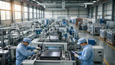
Advanced Packaging Equipment Growth Outpaces Front-End Equipment for the First Time
Advanced Packaging Equipment Growth Outpaces Front-End Equipment for the First Time
For decades, the center of gravity in semiconductor capital spending has lived squarely in the front end of the line—lithography, etch, deposition, and other wafer‑fab tools. Packaging was often treated as an afterthought: necessary, but secondary. That hierarchy is now changing. For the first time, growth in advanced packaging equipment is outpacing growth in traditional front end equipment, signaling a structural shift in how performance, cost, and innovation are created in the chip industry.
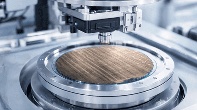
This blog post explores why advanced packaging has become the fastest‑growing segment of semiconductor equipment, what technologies and business drivers sit behind that inflection, and what it means for fabs, OSATs, equipment makers, and investors. The rise of advanced packaging marks a broader transition from “faster transistors” to “better systems,” and capital flows are beginning to reflect that reality.
From back end afterthought to strategic growth engine
Traditional semiconductor manufacturing divides into front end (wafer fabrication) and back end (assembly, test, and packaging). Historically, front end investments dominated, driven by node shrinks and the pursuit of Moore’s Law. Packaging focused on protecting and connecting chips—wire bonding, basic substrates, and housings.
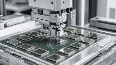
Advanced packaging breaks that old mold. Techniques such as flip‑chip, wafer‑level packaging, 2.5D interposers, 3D stacking, and chiplet‑based integration turn packaging into an active performance enabler. Instead of merely enclosing a die, advanced packages provide high‑bandwidth, low‑latency connections between multiple dies, mix different process nodes, and optimize power and form factor.
As these techniques become central to system design, the equipment that enables them—bumpers, bonders, molders, test handlers, and advanced substrate processing tools—moves from peripheral capex to strategic growth spending.
Why advanced packaging demand is accelerating
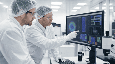
The core driver of advanced packaging equipment growth is the shift in how performance is scaled. Front end scaling has grown more expensive and difficult at cutting‑edge nodes. While leading fabs still invest heavily in EUV lithography and advanced process tools, the incremental performance gains per dollar are no longer as straightforward as they once were.
System designers therefore increasingly look to package‑level innovation: combining multiple chips in tight proximity, using high‑density interconnects, and optimizing the physical layout of compute, memory, and I/O. Advanced packaging allows mixing nodes (e.g., bleeding‑edge logic with more mature analog or RF), creating heterogeneous systems that maximize performance per watt and per dollar.
This architectural shift translates directly into equipment demand. The more systems rely on complex multi‑die integration, the more capacity and sophistication packaging lines need—and capex budgets follow.
Chiplets and disaggregation: fuel for packaging growth
The rise of chiplet‑based design exemplifies why advanced packaging is in ascendance. Instead of building increasingly larger monolithic dies, designers split functionality into smaller dies (“chiplets”) manufactured on optimal process nodes and then assemble them in a single package with high‑speed interconnects.
This disaggregation reduces yield risk and can lower costs, but it requires highly capable packaging. Fine‑pitch bumping or hybrid bonding, precision placement, and advanced substrates are essential to ensure that chiplets communicate as if they were part of a single monolithic die.
As more CPU, GPU, and accelerator vendors adopt chiplet strategies, the volume of packages needing sophisticated assembly rises sharply. Equipment for bumping, bonding, underfill, thermal management, and test must scale accordingly, driving packaging‑equipment growth faster than incremental front end tool expansion.
High‑bandwidth memory and advanced interposers
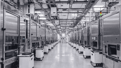
High‑bandwidth memory (HBM) has become a cornerstone of AI accelerators and high‑end compute. HBM stacks DRAM dies vertically and connects them to logic through wide, fast interfaces, typically via silicon interposers or other advanced packaging schemes.
Producing HBM requires specialized equipment: through‑silicon via (TSV) formation, wafer thinning, microbump formation, precision 3D stacking, and high‑density interposer fabrication. Each of these steps adds new categories of tools to packaging lines, significantly expanding capital requirements beyond traditional wire bonding and encapsulation.
The explosive growth of AI workloads and demand for HBM‑equipped accelerators amplifies this effect. As more systems adopt HBM, advanced packaging equipment becomes a bottleneck and a core growth vector, surpassing incremental front end expansions in some periods.
System‑in‑package and heterogeneous integration
System‑in‑package (SiP) approaches integrate diverse functions—logic, memory, RF, sensors, power management—into a single package. Instead of a single SoC handling everything, multiple optimized dies cooperate within a compact footprint.
Heterogeneous integration of this kind requires sophisticated assembly: multiple die attach techniques, varied interconnect styles, complex substrates, and careful thermal and mechanical design. Equipment for multi‑die placement, fine‑pitch interconnect, over‑molding, and high‑coverage test all see rising demand.
Because heterogeneous systems are proliferating across mobile, automotive, and IoT devices, SiP‑related equipment growth extends beyond high‑end compute, broadening the base of advanced packaging capex and reinforcing its lead over front end growth rates.
OSAT transformation: from low‑margin assembly to technology partners
Outsourced semiconductor assembly and test (OSAT) providers have traditionally occupied lower‑margin positions in the value chain, handling conventional packaging and final test. The rise of advanced packaging is reshaping their role.
Many OSATs are investing heavily in advanced packaging capabilities—fan‑out wafer‑level packaging, 2.5D and 3D integration, embedded bridge technologies—to serve fabless companies and even foundries seeking flexible packaging options. These investments show up directly in equipment orders, shifting OSAT capex profiles toward more complex tools.
As OSATs become technology partners rather than simple assemblers, the ratio of packaging equipment spending to front end tool spending moves upward, especially in regions where front end fab construction is constrained but packaging expansion remains relatively flexible and capital‑efficient.
Economics: where incremental value is highest
Part of the reason advanced packaging equipment growth outpaces front end is economic: packaging can deliver significant system‑level value at lower incremental cost than another node shrink. Moving from one front end node to the next often requires billions in fab and tool investments for modest performance and density gains.
In contrast, investing tens or hundreds of millions in advanced packaging capacity can unlock new architectures—chiplets, HBM, SiP—that yield substantial improvements in bandwidth, latency, power efficiency, and system flexibility. The ROI per dollar of capex can be compelling.
This economic logic encourages both foundries and fabless designers to allocate more capex to advanced packaging equipment. Over time, the capital mix shifts, and growth rates reflect where the next big gains in value are being realized: increasingly at the package level.
Technology convergence: front end and back end blur
Advanced packaging also blurs the traditional boundary between front end and back end. Some cutting‑edge packaging steps, such as hybrid bonding, TSV formation, or certain wafer‑level processes, resemble front end operations and may even occur in cleanroom environments.
This convergence means that some “packaging” equipment looks and behaves more like front end tools, with similar complexity, precision, and capital intensity. Nonetheless, they sit on the packaging side of the ledger in accounting terms, contributing to the observed faster growth of packaging‑classified equipment.
As more processes migrate to wafer‑level and 3D integration, the share of capital counted under advanced packaging categories naturally grows, even though the underlying technology draws heavily from front end experience.
Regional and policy drivers
Regional initiatives to build semiconductor ecosystems often emphasize front end fabs, but advanced packaging plants are sometimes easier to establish and less exposed to the most stringent technology restrictions. Governments seeking to increase local semiconductor content may find packaging investments more accessible in the near term.
Supportive policies—tax incentives, grants, and infrastructure support—for packaging facilities encourage equipment orders for bumping lines, substrate factories, and assembly/test equipment. These initiatives can cause packaging equipment growth to surge ahead of front end tool growth in certain regions, reinforcing the global trend.
As packaging capabilities become recognized as strategic assets, policy emphasis may further tilt toward advanced packaging, sustaining elevated growth rates relative to front end capex over multiple years.
Implications for equipment vendors
Equipment vendors are adapting their strategies to the new reality. Companies with strong packaging portfolios—bonders, molders, wafer‑level packaging tools, test handlers—see growing opportunities and invest in capacity and R&D. Front end tool vendors explore adjacent packaging markets (e.g., wafer‑level bonding, TSV tools) to participate in advanced integration trends.
As packaging equipment growth outpaces front end, vendors may rebalance their R&D budgets and sales focus, pursuing technologies that enable chiplet assembly, HBM integration, and SiP manufacturing. Partnerships with OSATs and foundries around co‑developed packaging flows become more important.
For vendors, the shift underscores that long‑term leadership in semiconductors now requires excellence beyond the wafer—into how dies are combined, connected, and tested at the package level.
Implications for fabs, OSATs, and designers
For fabs and OSATs, the relative growth of packaging equipment means that packaging capacity and capability are increasingly critical differentiators. Advanced packaging lines can become bottlenecks if not expanded in step with front end production.
Chip designers must now consider packaging early in architecture decisions, ensuring that their performance goals align with available packaging technologies and capacities. Close collaboration between design teams and packaging engineers, as well as with equipment vendors, is necessary to realize the full benefits of advanced integration.
This tighter integration across the value chain—design, front end, packaging, and test—reshapes planning and investment cycles, with packaging no longer a late‑stage consideration but a co‑equal pillar of product strategy.
Investor perspective: reweighting the semi equipment universe
Investors tracking semiconductor equipment markets need to account for the changing balance between front end and packaging. Historically, front end tool makers captured most of the “growth” narrative, while packaging equipment was seen as more incremental.
Now, advanced packaging stands out as a structural growth theme tied to AI, high‑performance computing, mobile, automotive, and IoT systems. Equipment firms positioned in bumping, wafer‑level packaging, bonding, advanced substrates, and test can see higher growth trajectories and potentially different valuation profiles than purely front end players.
Portfolio construction and thematic strategies increasingly consider advanced packaging exposure as a key dimension, reflecting the reality that system performance is as much about how chips are assembled and connected as how transistors are etched and deposited.
Looking ahead: sustained outperformance or cyclical spike?
The question naturally arises: is the current outperformance of advanced packaging equipment growth over front end growth a temporary spike or a sustained structural shift? Several factors suggest it is more structural than cyclical.
Architectural trends—chiplets, HBM, SiP, heterogeneous integration—are set to continue, driven by fundamental limits in monolithic scaling and systemic performance demands. These trends inherently rely on advanced packaging. At the same time, the economic calculus favors packaging innovation as a relatively efficient way to deliver system‑level gains.
While cycles and macro conditions will undoubtedly affect absolute spending levels, the relative importance of advanced packaging is likely to remain elevated. That implies that packaging equipment growth outpacing front end growth could be a recurring feature of future investment cycles, not a one‑off anomaly.
Conclusion: a new balance in semiconductor capital spending
The fact that advanced packaging equipment growth is outpacing front end equipment growth for the first time marks a turning point in semiconductor capital allocation. It reflects a broader shift in where innovation and value are being created—from ever smaller transistors alone to smarter ways of integrating and connecting multiple chips.
As advanced packaging becomes central to performance, power, and cost, the tools that enable it move to the forefront of investment decisions. For the industry, this new balance means that leadership will be defined not only by front end process prowess, but also by mastery of the package as a system‑level platform. For those watching capex trends, the message is clear: the future of semiconductor progress is increasingly being built not just in the fab’s front end, but on the intricate stages of advanced packaging lines.