
Hot Posts
2027 SOX Target Price: The Sell-Side Divergence Summary
A 2027 target for the Philadelphia Semiconductor Index looks precise: one number, one horizon, one implied return. Underneath that number, however, sit several competing forecasts. How long can AI investment accelerate? When does memory supply catch demand? Will industrial chips recover? And what valuation will investors pay when those earnings finally arrive?Applied Materials’ FY26 Q4 Revenue Beat: The Equipment Supercycle Evidence
Applied Materials’ fiscal 2026 fourth-quarter revenue beat cannot yet be evaluated as a completed event. As of October 9, 2026, the company’s latest reported quarter was fiscal Q3, and its investor presentation listed November 12 as the projected date for its Q4 earnings call. What exists today is a strong reported quarter and an ambitious forward outlook—not an announced Q4 result.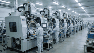
Equipment Order Backlog Visibility: Why 2027 Deliveries Are Already Booked
For selected semiconductor equipment suppliers, 2027 is already taking shape inside the order book. Customers are reserving systems before the delivery year begins, manufacturers are allocating production capacity, and component suppliers are preparing for schedules that extend beyond the next quarterly earnings report.Advanced Packaging Material Demand: Underfill and TIM Localization
A large AI package can contain exceptional silicon and still fail because a relatively inexpensive material does not behave as expected. An underfill that leaves voids can compromise interconnect reliability. A thermal interface material that loses contact can turn an acceptable cooling design into a temperature problem.Wafer Edge Polishing Equipment: The SOI Substrate Demand Driver
The center of a semiconductor wafer receives most of the attention. That is where engineers measure film thickness, pattern devices, and evaluate electrical performance. The edge looks less productive: a narrow perimeter that cannot accommodate complete dies and often sits outside the usable processing area.Indices

Storage
NAND Layer Count Race: Kioxia’s 332-Layer BiCS10 Sample Delivery
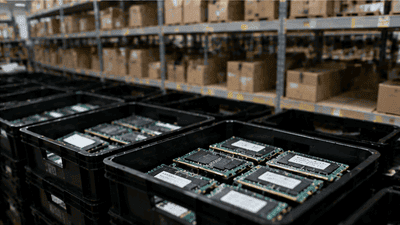
Kioxia’s 332-layer BiCS10 NAND marks a meaningful step in the race to build denser, faster, and more power-efficient flash memory. Yet the most important word in the announcement is not “332.” It is “samples.” The technology has reached functional evaluation, while its commercial significance still depends on manufacturing execution and integration into qualified storage products.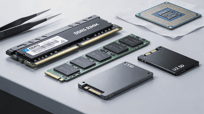
Equipment
Applied Materials’ FY26 Q4 Revenue Beat: The Equipment Supercycle Evidence
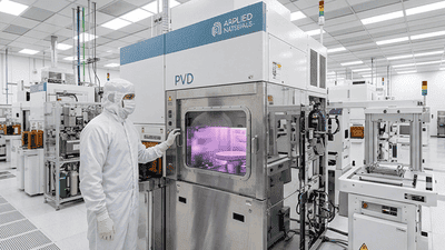
Applied Materials’ fiscal 2026 fourth-quarter revenue beat cannot yet be evaluated as a completed event. As of October 9, 2026, the company’s latest reported quarter was fiscal Q3, and its investor presentation listed November 12 as the projected date for its Q4 earnings call. What exists today is a strong reported quarter and an ambitious forward outlook—not an announced Q4 result.
Advanced Packaging

The Three-Headed Race in Advanced Packaging: TSMC, Intel, and ASE
For years, chip conversations revolved around transistor nodes and wafer fabs. Today, the more interesting battles are often happening a few millimeters above the silicon, in the world of advanced packaging. As AI, high‑performance computing, and high‑bandwidth memory redefine what a “chip” looks like, three names stand out in the packaging race: TSMC, Intel, and ASE. Each comes from a different starting point, with different strengths and weaknesses, and together they’re reshaping how heterogeneous integration will be done for the next decade.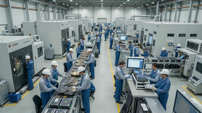
Competitive Landscape of Advanced Packaging: The Coopetition Between OSATs and Foundries
Advanced packaging has moved from the back end of semiconductor manufacturing to the center of the industry’s strategic map. As AI, high-performance computing, mobile systems, automotive electronics, and chiplets all push toward heterogeneous integration, one question has become unavoidable: who owns the packaging layer of the future, OSATs or foundries? The answer is not a clean winner-takes-all outcome. It is a complex and evolving contest of overlap, specialization, and cooperation. In other words, it is cooptition.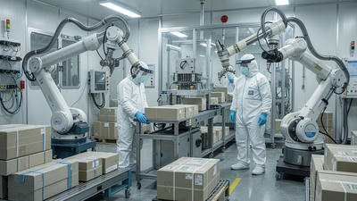
New Standards for Cleanroom Grades and Environmental Requirements in Advanced Packaging
Advanced packaging has changed the rules of semiconductor manufacturing, and cleanroom standards are changing with it. What used to be a largely front-end concern is now a packaging concern too, because heterogeneous integration depends on much more than just transistor quality. It depends on the cleanliness of bonding surfaces, the stability of thin wafers, the behavior of mold compounds, the integrity of fine-pitch interconnects, and the control of particles, humidity, and temperature throughout assembly. In short, the environment has become part of the design.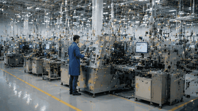
ASE and Amkor’s 2026 CapEx Priorities – Advanced Packaging Focus
If 2025 was the year the market finally accepted that advanced packaging was no longer a niche, 2026 is the year ASE and Amkor are acting like it. Both companies are putting capital behind the same big idea: advanced packaging and heterogeneous integration are now central growth engines, not side businesses. The scale of their spending plans says as much as any earnings call or roadmap slide. In a market reshaped by AI, HPC, chiplets, and HBM, CapEx has become a statement of strategy.Materials
-
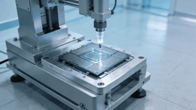 A large AI package can contain exceptional silicon and still fail because a relatively inexpensive material does not behave as expected. An underfill that leaves voids can compromise interconnect reliability. A thermal interface material that loses contact can turn an acceptable cooling design into a temperature problem.
 -
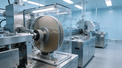 The center of a semiconductor wafer receives most of the attention. That is where engineers measure film thickness, pattern devices, and evaluate electrical performance. The edge looks less productive: a narrow perimeter that cannot accommodate complete dies and often sits outside the usable processing area.
 -
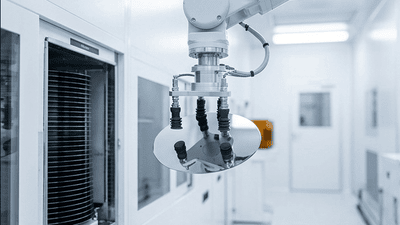 The silicon wafer market is recovering in 2026, but the recovery is neither uniform nor adequately explained by the artificial intelligence investment boom alone. Shipment area is increasing, advanced applications remain the strongest demand engine, and industrial and automotive markets are showing signs of improvement. Yet rising volumes do not automatically imply stronger pricing, fully utilized factories, or an equally healthy outlook across wafer categories.
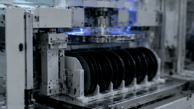
 -
 The semiconductor industry is entering a critical transition period as silicon carbide (SiC) technology moves from a specialized material platform toward broader commercial adoption. Once considered an expensive alternative semiconductor material, SiC is rapidly gaining importance in electric vehicles, renewable energy systems, industrial power equipment, and high-efficiency power electronics. A major factor determining the speed of adoption will be the continued decline of SiC substrate costs.