Recycling and Circularity of Semi Materials (Green Silicon) as an ESG Investment Theme
Recycling and Circularity of Semi Materials (Green Silicon) as an ESG Investment Theme
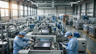
Semiconductor manufacturing sits at the crossroads of technological progress and environmental scrutiny. As demand for chips soars—driven by AI, mobile devices, electric vehicles, and IoT—so do the material flows, energy consumption, and waste streams that underpin fabrication. "Green silicon" and broader circular approaches for semiconductor materials are emerging as crucial elements of environmental, social, and governance (ESG) investment strategies. This article explains why recycling and circulation of semiconductor materials matter, outlines the main technical and market levers, highlights key risks and opportunities for investors, and offers practical frameworks for integrating these themes into ESG-focused portfolios.
Why semiconductor material circulation is an ESG priority
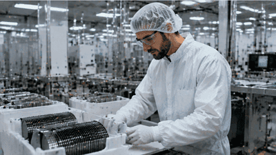
Three core trends make semiconductor material recycling and circulation an urgent ESG priority:
- Rising material intensity: Advanced chips rely on highly refined materials—silicon wafers, specialty gases, rare metals, and chemicals. High-volume manufacturing multiplies the total resource footprint.
- Energy and emissions profile: Fabrication (fabs) is energy-intensive. The upstream production of materials (e.g., polysilicon crystallization, wafer slicing, chemical synthesis) further contributes to greenhouse gas emissions and water use.
- Waste and critical-material risk: Manufacturing yields, end-of-life electronics, and obsolete inventory generate hazardous waste streams and create demand for critical or scarce materials (e.g., palladium, indium, tantalum). Reliance on constrained supply chains raises geopolitical and supply-risk concerns.
Addressing these issues through recycling, reclamation, and circular material flows reduces environmental impact, improves supply security, and aligns semiconductor producers and suppliers with evolving regulatory and customer expectations—making it a compelling ESG investment theme.
What is "green silicon" and what does circulation mean?
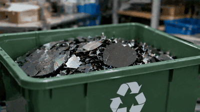
"Green silicon" refers broadly to silicon and silicon-based processes produced and managed in ways that minimize environmental harm and maximize resource efficiency. That includes:
- Low-carbon polysilicon production, powered by renewable energy and optimized processes.
- Reduced water and chemical usage during wafer fabrication and wet processes.
- Reclaimed silicon and wafer recycling—turning scrap wafers, kerf (sawmill) loss, and end-of-life silicon back into usable feedstock.
- Closed-loop material flows where solvents, process gases, and etchants are recovered and reused.
Circulation extends beyond silicon: it covers reclamation of specialty chemicals, recovery of rare metals from scrap, refurbishment and reuse of equipment, and design-for-recycling strategies that make end-of-life recovery easier. Together, these actions form a circular value chain in which waste is minimized and materials remain in productive use longer.
Technical pathways for semiconductor material recycling
Recycling in the semiconductor industry operates at multiple life-cycle stages. Major technical avenues include:
1. Wafer and silicon recovery
- Kerf loss reduction and recycling: Traditional wafer slicing with sawing wastes a fraction of the silicon (kerf). Newer diamond-wire sawing and kerfless wafering reduce waste. Kerf slurry and sawdust can be chemically processed to recover silicon particles for reprocessing into polysilicon or lower-grade feedstock.
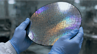
- Reclaiming scrap wafers: Defective or test wafers can be chemically stripped of films and dopants, then polished and repolished into usable substrates. Advanced chemical-mechanical polishing (CMP) reclaim processes are improving yield of reclaimed wafers.
2. Chemical and solvent recovery
- Closed-loop solvent recycling: High-purity solvents and process chemicals used in wet benches and cleaning can be distilled and purified for reuse, reducing both procurement and hazardous waste disposal.
- Etchant and slurry recovery: Technologies separate usable components from spent etchants and CMP slurries, enabling recovery of water, acids, and abrasive materials.
3. Specialty gas capture and reuse
- Recovery systems capture fluorinated greenhouse gases and specialty process gases; these can be purified or destroyed via abatement. On-site recycling systems help reduce net emissions and operating cost exposure to volatile gas prices.
4. Critical-metal reclamation
- End-of-life electronics and scrap from fabs contain palladium, platinum, gold, indium, and other critical elements. Hydrometallurgical and pyrometallurgical processes selectively recover these metals for re-introduction to supply chains.
5. Equipment refurbishment and remanufacturing
- Capital equipment (CMP tools, lithography aligners, thermal furnaces) has significant embedded carbon and materials. Refurbishing and remanufacturing extend equipment life, lower capital demand, and reduce the environmental footprint of fabs.
Market and policy drivers accelerating green semiconductor materials

Several external pressures are creating tailwinds for circular semiconductor material solutions:
- Regulatory tightening: Regions are increasing restrictions on hazardous waste, water discharge, and greenhouse gas emissions. Extended producer responsibility (EPR) frameworks may make manufacturers accountable for end-of-life disposal, incentivizing design-for-recycling and takeback programs.
- Corporate procurement and customer demand: OEMs and hyperscalers increasingly require suppliers to meet sustainability criteria. Buyers prefer chips and materials with documented lower carbon and circularity footprints.
- Supply-chain resilience strategies: Concerns about geopolitical concentration of material refining (e.g., rare earths) push companies and governments to favor domestic recycling and circular capacity to reduce import dependency.
- Cost pressures and resource scarcity: Recovered materials can insulate manufacturers from commodity price volatility and reduce overall production costs when recovery processes are scaled efficiently.
Investment thesis: Why green silicon is an attractive ESG theme
For ESG-minded investors, green silicon and semiconductor material circulation present multiple avenues to generate both impact and returns:
- High impact potential: Improvements in wafer recycling, energy sourcing, and chemical recovery can meaningfully reduce the industry’s carbon intensity and hazardous waste—offering measurable ESG outcomes.
- Structural demand growth: As global chip demand continues expanding, the absolute scale of materials used will grow—creating a large addressable market for recycling technologies and services.
- Regulatory-driven revenue upside: Firms providing recycling, abatement, and reclamation services may benefit from new compliance requirements and potential subsidies or tax incentives for clean manufacturing.
- Diversification and risk mitigation: Investments in domestic or regional circular capacity reduce exposure to geopolitically concentrated raw material suppliers, enhancing portfolio resilience.
- Innovation premium: Early investors in breakthrough recycling or low-carbon production technologies can capture outsized returns if those technologies become industry standards.
Where to invest: segments and examples
Investors can participate across a value chain spanning raw-material producers to waste processors and enabling technologies. Key segments include:
- Low-carbon polysilicon producers: Companies that use renewable energy and efficient processes to produce polysilicon for wafers and PV, often overlapping with solar supply chains.
- Wafer reclaim and kerf-recovery specialists: Firms that convert sawdust, slurry, and defective wafers into feedstock or reusable substrates.
- Chemical recycling and solvent recovery providers: Service companies and equipment makers that install closed-loop purification systems in fabs.
- Gas abatement and specialty gas recyclers: Providers of capture, purification, and abatement solutions for fluorinated and process gases.
- Materials recyclers and refiners: Hydrometallurgical firms that recover precious and rare metals from scrap electronics and fab waste.
- Refurbishers and remanufacturers of equipment: Businesses that refurbish lithography, CMP, and thermal tools to extend asset life.
- Software and analytics: Startups offering lifecycle assessment (LCA), circularity analytics, and traceability platforms that enable buyers to verify "green" claims.
Public equities, private venture and growth capital, green bonds, and project-level financing each provide routes to gain exposure depending on risk tolerance and time horizon.
Metrics and due diligence for ESG investors
Evaluating companies in this space requires a blend of technical scrutiny and sustainability assessment. Key metrics include:
- Material recovery rates: Percentage of silicon, metals, or chemicals successfully reclaimed versus processed waste.
- Scope 1–3 emissions and intensity: Absolute and per-unit greenhouse gas emissions across manufacturing and upstream material production, reported transparently and audited where possible.
- Water use and effluent quality: Water consumption per wafer and the quality of treated wastewater discharged.
- Energy sourcing: Share of energy from renewables, presence of long-term power purchase agreements (PPAs), and on-site generation.
- Regulatory compliance and permits: Track record of environmental compliance and readiness for stricter future standards.
- Supply-chain traceability: Ability to demonstrate provenance of reclaimed materials and ensure material quality meets semiconductor-grade specifications.
- Economic viability: Cost per kilogram of recovered material, capex/opex requirements for recycling systems, and expected payback periods.
Qualitative diligence should include management competence in scaling recycling operations, partnerships with fabs and OEMs for off-take, IP and process defensibility, and engagement with regulators and certification bodies.
Challenges and counterpoints
While promising, the green silicon and circulation theme faces practical obstacles:
- Quality and purity requirements: Semiconductor production demands extremely high-purity materials. Achieving semiconductor-grade quality from recycled feedstock can be technically challenging and costly.
- Economics at scale: Recovery processes must be efficient enough to compete with primary production costs. For some materials, primary refining remains cheaper, especially where cheap energy or feedstock subsidies exist.
- Fragmented waste streams: End-of-life electronics and fab wastes are dispersed and sometimes contaminated, raising collection and sorting costs.
- Regulatory complexity: Differing global regulations on hazardous waste movement and recycling can complicate cross-border circular solutions.
- Verification and greenwashing risk: Without robust standards and third-party verification, some "green" claims may be overstated, undermining investor and customer trust.
How investors can structure exposure
Investors can use several strategies to gain exposure while managing risk:
- Diversified thematic funds: Invest via funds focused on sustainable materials, clean manufacturing, or circular economy solutions to spread technology and company risk.
- Direct equity in specialists: Select leaders in polysilicon, wafer reclaim, or gas abatement with proven customers and scalable processes.
- Private deals and venture capital: Back early-stage companies developing breakthrough recycling technologies, with staged funding tied to technical milestones.
- Project finance and green bonds: Fund capex for on-site recycling installations at fabs, or refinance refurbishment projects with sustainability-linked instruments.
- Engagement and stewardship: For shareholders of fabs and semiconductor suppliers, use active engagement to push for circularity targets, disclosure improvements, and investments in reclaim capacity.
Case study (illustrative)
Consider a mid-sized wafer reclamation company that partners with regional fabs to collect kerf slurry and defective wafers. By investing in a chemical extraction line and ultrasonic cleaning stations, the company increases silicon recovery from 40% to 80% at an incremental cost that is lower than new polysilicon on a per-kg basis when accounting for avoided waste disposal fees and carbon penalties. The firm locks in supply contracts with three fabs and signs an offtake agreement with a domestic polysilicon producer seeking lower-carbon feedstock. Investors benefit from a predictable revenue stream, strong ESG metrics (reduced landfill and scope 3 emissions for partner fabs), and a defensible position because of proprietary purification techniques and fab integration. This kind of vertically integrated model demonstrates how economic returns and material impact can align.
Policy and standardization needs
To scale circularity across the semiconductor industry, several systemic enablers are necessary:
- Standardized metrics and certification: Industry-wide LCA methodologies and certification programs for "green" materials will reduce verification costs and limit greenwashing.
- Incentives and subsidies: Government support for domestic recycling capacity—through grants, tax incentives, or guaranteed procurement—can lower the hurdle for capital-intensive recycling plants.
- Trade and waste frameworks: Harmonized regulations for cross-border movement of e-waste and hazardous process waste will enable centralized recycling hubs while maintaining environmental safeguards.
- Public–private partnerships: Coordinated initiatives between fabs, recyclers, and research institutions can accelerate pilot projects and commercial deployment of new recovery technologies.
Outlook and investment timeline
In the near term (2–5 years), investors should expect incremental adoption: solvent recycling, gas abatement upgrades, and pilot reclaim programs at scale in mature markets. Mid-term (5–10 years), mature circular technologies—improved kerf recovery, higher-yield wafer reclamation, and broader precious-metal recovery—could reach commercial parity in many regions, driven by regulation and falling technology costs. Long-term (10+ years), if systemic policy support and standardized certification emerge, circular material flows could become a conventional component of fab supply chains, enabling lower emissions and more resilient supply models.
Practical checklist for investors
Use this checklist when evaluating opportunities:
- Verify material purity targets and independent test results for reclaimed products.
- Assess customer contracts with fabs or OEMs—are there binding off-take or pilot agreements?
- Evaluate capex needs and path to scale: Is the business unit economics-driven at commercial volumes?
- Check regulatory positioning: Does the company meet current permits and anticipate future compliance costs?
- Review management and technical talent with domain experience in semiconductor processes.
- Request clear ESG KPIs (recovery rates, emissions avoided, water saved) and audit mechanisms.
Conclusion
Recycling and circulation of semiconductor materials—epitomized by the "green silicon" concept—represent a growing, multifaceted ESG investment theme. The combination of environmental benefit, supply-chain resilience, and regulatory momentum creates a fertile environment for investors seeking both impact and returns. Success will hinge on technical execution, credible measurement, and supportive policy frameworks. For investors, the most attractive opportunities balance demonstrable recovery yields and scalable economics with strong customer relationships and transparent ESG reporting.
As chip demand continues to rise, circular approaches will shift from nice-to-have to strategic imperatives. Early, disciplined investment in technologies, service providers, and business models that enable semiconductor material circulation can capture value while contributing to a lower-carbon, more resilient electronics ecosystem.