Wafer Size Battle: 300mm Demand Share Continues to Rise, 200mm Stabilizes
The semiconductor industry has always been defined by continuous technological advancement, and wafer size evolution remains one of the most important drivers of manufacturing efficiency. Over the past two decades, the transition from 200mm wafers to 300mm wafers has reshaped semiconductor production economics by enabling higher output, improved cost efficiency, and greater manufacturing scalability. As global demand for advanced computing, artificial intelligence, automotive electronics, and industrial semiconductors continues to expand, the balance between 300mm and 200mm wafer demand is becoming a critical topic across the semiconductor supply chain.
While 300mm wafers are steadily increasing their share of global semiconductor production due to their advantages in productivity and cost reduction, 200mm wafers remain an essential part of the industry. Mature process technologies, specialty semiconductors, power devices, analog chips, sensors, and automotive components continue to rely heavily on 200mm manufacturing platforms. Instead of completely replacing older wafer sizes, the semiconductor industry is moving toward a more diversified manufacturing structure where both wafer formats serve different market requirements.
The ongoing wafer size battle is therefore not a simple competition between old and new technologies. It represents a strategic balance between advanced manufacturing efficiency and long-term demand for mature semiconductor applications.
The Evolution of Semiconductor Wafer Sizes
Semiconductor manufacturing has historically progressed through several wafer size transitions. Early semiconductor production relied on smaller wafer formats, including 100mm and 150mm wafers. As manufacturing technology improved, the industry moved toward 200mm wafers during the 1990s, followed by the widespread adoption of 300mm wafers in the early 2000s.
The primary motivation behind increasing wafer size is economic efficiency. A larger wafer allows semiconductor manufacturers to produce more chips during each fabrication cycle. Since many manufacturing steps, such as deposition, lithography, etching, and inspection, are performed at the wafer level, processing more dies simultaneously reduces the average cost per chip.
A 300mm wafer provides approximately 2.25 times the surface area of a 200mm wafer. Although larger wafers require more advanced manufacturing equipment and higher capital investment, the increased number of chips per wafer creates significant cost advantages, especially for high-volume semiconductor products.
As semiconductor demand has shifted toward increasingly complex chips, wafer size has become closely connected with manufacturing strategy. Leading-edge logic processors and memory devices have largely migrated toward 300mm production, while many specialty semiconductor markets continue to depend on 200mm fabs.
Why 300mm Wafer Demand Continues to Grow
The strongest driver behind the continued expansion of 300mm wafer demand is the growth of high-performance semiconductor applications. Artificial intelligence, cloud computing, data centers, and advanced consumer electronics require chips with higher performance and greater transistor density. These applications are typically manufactured using advanced process technologies that rely on 300mm wafer platforms.
Memory manufacturers have been among the biggest users of 300mm wafers. DRAM and NAND flash production benefit significantly from larger wafer sizes because memory products are manufactured in extremely high volumes. Lower manufacturing costs directly improve competitiveness in highly price-sensitive memory markets.
Advanced logic semiconductor production is another major contributor. Companies developing processors, artificial intelligence accelerators, and high-performance computing chips increasingly depend on advanced 300mm fabrication facilities. These fabs provide the precision control, automation level, and process capability required for cutting-edge semiconductor manufacturing.
Another important factor is factory automation. Modern 300mm fabs are designed around highly automated material handling systems, advanced process control, and digital manufacturing technologies. This allows manufacturers to achieve higher productivity and more consistent wafer quality.
The Economic Advantages of 300mm Manufacturing
The transition to 300mm wafers has fundamentally changed semiconductor manufacturing economics. The cost advantage comes from several factors, including higher wafer output, improved equipment utilization, and reduced labor requirements.
Because each 300mm wafer contains more semiconductor dies than a 200mm wafer, manufacturers can spread fixed production costs across a larger number of chips. This becomes particularly valuable for products with large production volumes, where even small cost reductions can significantly improve profitability.
In addition, newer 300mm fabs often incorporate advanced manufacturing technologies from the beginning. These facilities are typically built with higher levels of automation and optimized production flows, improving overall efficiency.
For semiconductor companies competing in global markets, manufacturing cost advantages are becoming increasingly important. As chip complexity rises and development expenses increase, efficient wafer production becomes a major factor influencing competitiveness.
Why 200mm Wafers Remain Important
Despite the growth of 300mm manufacturing, 200mm wafers continue to play a crucial role in the semiconductor industry. Many semiconductor products do not require the newest process technologies and are better suited to mature manufacturing platforms.
Analog semiconductors are one of the largest markets supported by 200mm fabs. These chips are widely used in automotive systems, industrial equipment, power management applications, and consumer electronics. Their manufacturing requirements are different from advanced processors, focusing more on reliability, performance consistency, and specialized functionality.
Power semiconductors also remain heavily dependent on 200mm production. Devices used in electric vehicles, renewable energy systems, and industrial power applications often require specialized processes that are not easily transferred to advanced 300mm platforms.
Additionally, many semiconductor manufacturers have invested billions of dollars in existing 200mm facilities. These fabs continue to generate strong returns because they produce mature technologies with stable demand.
The Stabilization of 200mm Wafer Demand
After years of declining attention compared with 300mm expansion, the 200mm wafer market has entered a period of stabilization. Several structural factors support continued demand for 200mm manufacturing capacity.
The growth of automotive electronics is one major reason. Modern vehicles contain hundreds or even thousands of semiconductor components, including sensors, power management chips, microcontrollers, and communication devices. Many of these components rely on mature semiconductor processes manufactured on 200mm wafers.
The expansion of industrial automation and smart infrastructure is another important factor. Industrial applications often prioritize long-term reliability rather than the smallest possible semiconductor size. As a result, mature manufacturing technologies remain highly valuable.
Supply chain diversification has also increased interest in 200mm capacity. Semiconductor companies and governments are seeking additional manufacturing flexibility to reduce dependence on limited production sources. Existing 200mm fabs provide a practical option for expanding semiconductor supply without requiring the enormous investment needed for advanced 300mm facilities.
Capacity Challenges in the 300mm Market
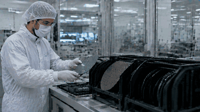
Although 300mm demand continues to rise, expanding capacity is not simple. Building a new 300mm semiconductor fabrication facility requires significant capital investment, advanced equipment, and a highly skilled workforce.
The cost of constructing an advanced semiconductor fab can reach billions of dollars. Beyond the building itself, manufacturers must invest in lithography equipment, process tools, cleanroom infrastructure, and complex manufacturing systems.
Equipment availability is another challenge. Advanced semiconductor manufacturing equipment has long delivery cycles, and demand from global chip manufacturers can exceed supplier capacity.
These challenges create a situation where demand for 300mm production may continue growing faster than new capacity can be added. As a result, semiconductor manufacturers are carefully planning investments to ensure sufficient future supply.
The Role of Regional Semiconductor Expansion
The global semiconductor industry is experiencing a major wave of regional investment. Governments and companies across North America, Europe, and Asia are investing in domestic semiconductor manufacturing capabilities.
This trend is influencing wafer size strategies. New advanced fabs are generally built around 300mm wafer technology because companies want to maximize long-term efficiency and competitiveness.
At the same time, regional manufacturing expansion is also supporting 200mm capacity. Many countries need reliable supplies of automotive, industrial, and specialty semiconductors, creating demand for mature-node production facilities.
The result is a more balanced semiconductor ecosystem where both wafer sizes continue to have strategic importance.
The Impact on Semiconductor Equipment and Materials Suppliers
The changing balance between 300mm and 200mm wafers has significant implications for semiconductor equipment and materials companies.
300mm expansion creates strong demand for advanced manufacturing equipment, automation systems, and high-performance semiconductor materials. Companies supplying lithography systems, deposition equipment, inspection tools, and advanced chemicals benefit from continued investment in new fabs.
Meanwhile, 200mm fabs create opportunities for suppliers providing mature-node equipment, refurbished tools, specialty materials, and process solutions. Because many 200mm fabs operate for decades, maintenance and upgrade markets remain attractive.
This dual demand structure allows semiconductor suppliers to participate across different segments of the industry.
Future Outlook: A Coexistence Strategy
The future semiconductor manufacturing landscape will likely not be dominated by a single wafer size. Instead, 300mm and 200mm platforms will coexist based on application requirements.
300mm wafers will continue gaining share in areas requiring high-volume production, advanced processing, and maximum cost efficiency. Artificial intelligence, advanced computing, and memory technologies will remain major drivers of 300mm expansion.
200mm wafers will maintain importance in specialized semiconductor markets where mature processes, reliability, and cost stability are more important than transistor scaling.
This coexistence reflects a broader transformation in the semiconductor industry. Modern electronics require a wide range of chips, from advanced processors to simple control devices. Each application requires a different manufacturing strategy.
Conclusion
The wafer size battle between 300mm and 200mm is not a competition where one technology completely replaces another. Instead, it represents the semiconductor industry's adaptation to diverse market demands.
300mm wafers are continuing to expand because they offer superior economics, higher productivity, and support for advanced semiconductor manufacturing. Meanwhile, 200mm wafers remain essential because they support mature, specialized, and rapidly growing semiconductor applications.
As artificial intelligence, automotive electronics, industrial automation, and digital infrastructure continue driving semiconductor demand, both wafer platforms will remain important components of the global chip ecosystem. The future semiconductor industry will depend not only on technological advancement but also on maintaining the right balance between manufacturing scale, flexibility, and supply chain resilience.