ASML’s High-NA EUV Triple Partnership: Intel, Samsung, TSMC’s Production Plans
High-numerical-aperture extreme ultraviolet lithography is moving from an engineering development into a manufacturing roadmap shared by the industry’s largest chipmakers. The transition is not happening on one schedule, however, and the commercial implications depend on recognizing those differences.
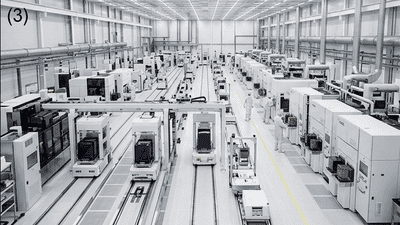
As of October 2026, Intel was already using High-NA EUV on selected production layers. Samsung had outlined adoption in high-volume DRAM manufacturing by 2028, while TSMC intended to introduce it into advanced-node high-volume manufacturing from 2030. These are distinct commitments, not three simultaneous factory conversions.
The “triple partnership” captures the importance of those customer relationships, but it should not imply one exclusive, identical agreement. A broader ecosystem is also involved in developing future capabilities. The central theme is sequencing: production experience today, additional adoption later, and subsequent infrastructure changes intended to improve long-term economics.
What High-NA Changes Technically
ASML’s conventional EUV platform uses a numerical aperture of 0.33. Its High-NA EXE platform increases that figure to 0.55, allowing the optical system to resolve finer patterns under the appropriate process conditions.
The improvement is not a change in the EUV wavelength. It is a change in the optical architecture and the way the system forms an image.
That distinction matters because better resolution brings additional requirements. Masks, resists, focus control, measurement, and manufacturing recipes must work with the new platform.
For a process engineer, High-NA is therefore not simply a brighter or faster version of an existing machine. It is a patterning option that needs to demonstrate value within a complete process flow.
Intel Has Moved Beyond Evaluation
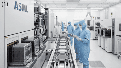
Intel’s September announcement described High-NA use in high-volume manufacturing on selected layers for a subset of its Core Ultra Series 3 processors, code-named Panther Lake.
The company also reported more than one million wafers processed across early tool certification, testing, research and development, and volume production. That total should not be presented as one million commercial production wafers.
This distinction preserves the significance of the achievement without exaggerating its scope. Intel has established production use, but not every Panther Lake product or every manufacturing layer has shifted to High-NA.
For equipment investors, the important development is that the technology has crossed a practical boundary: it is contributing to a commercial manufacturing flow rather than remaining solely a research instrument.
What Intel’s Early Adoption Can Provide
Operating experience can help a manufacturer learn how a new platform behaves under production conditions. Installation, maintenance, measurement, recipe stability, and defect investigation all generate information that is difficult to obtain from limited trials alone.
That experience can support future deployment. It does not automatically establish a permanent advantage over competitors.
The broader outcome depends on device performance, manufacturing yield, cost, customer demand, and the success of subsequent technology transitions. Lithography is one important part of that system.
From an analyst’s perspective, Intel’s early use is best understood as an opportunity to accumulate manufacturing knowledge. Whether that knowledge becomes a durable foundry advantage requires evidence beyond the initial High-NA milestone.
Samsung’s Dated Commitment Concerns DRAM

Samsung’s announced 2028 plan concerns high-volume DRAM manufacturing. It should not be rewritten as a promise that every Samsung foundry process or semiconductor product will use High-NA by that date.
Memory presents a distinct patterning context. Its structures, production economics, and technology transitions differ from those of leading-edge logic.
That gives Samsung a separate reason to evaluate the platform. The relevant question is how High-NA supports its intended memory process and whether the resulting benefit justifies the complete cost of adoption.
For investors, the distinction also changes the equipment thesis. A DRAM commitment creates a defined application pathway, but the timing of tool purchases, qualification, and production expansion still needs to be tracked independently.
TSMC’s 2030 Plan Reflects a Later Adoption Window
TSMC’s announced intention to begin advanced-node High-NA high-volume manufacturing from 2030 provides a clearer production direction than a general statement of interest.
It does not identify a universal conversion of TSMC’s factories, nor does it specify that every layer will require the technology. Assigning the rollout to an unannounced first node would go beyond the commitment.
A later adoption date should not automatically be interpreted as technological weakness. Manufacturers can choose different combinations of conventional EUV, patterning methods, and process development according to their economics and roadmaps.
From a factory manager’s perspective, the appropriate adoption point is when the platform provides sufficient manufacturing value—not merely when a competitor first uses it.
Three Schedules Create a Layered Equipment Opportunity

Intel’s existing use, Samsung’s memory plan, and TSMC’s later advanced-node plan create different stages of potential demand.
Current deployment can support service, applications work, and operational learning. Future adoption can generate evaluations and equipment commitments before production begins. Later infrastructure development can create another investment phase.
These stages should not be collapsed into immediate revenue. A production date is not necessarily an order date, and a customer commitment is not a disclosed unit count.
For ASML investors, the opportunity is broader customer participation over time. The uncertainty concerns the pace, scale, configuration, and economic performance of that participation.
The Larger-Mask Initiative Is a Separate Roadmap
Alongside production plans for existing High-NA technology, the ecosystem is developing a larger rectangular photomask format. The initiative targets a pilot line around 2031 and production-system readiness around 2033.
The format is commonly described as 6-by-12-inch masks, which is more precise than suggesting a circular twelve-inch mask. It addresses a later productivity and field-coverage opportunity, not a prerequisite for every earlier High-NA deployment.
This distinction is critical. Intel’s present production use and Samsung’s 2028 plan do not depend on waiting for that later initiative to reach its target dates.
The market therefore has two connected roadmaps: adoption of current High-NA systems and development of a subsequent configuration intended to improve their application range and economics.
Why Field Size Matters for Large Chips
Current High-NA optics introduce field-coverage constraints that are relevant to large designs. Depending on the implementation, customers need to consider design dimensions and possible stitching strategies.
That makes the issue particularly important for large compute devices. A resolution benefit needs to be evaluated alongside the practical task of patterning the intended design.
Larger-mask development seeks to address part of that challenge. However, changing mask format requires more than modifying one scanner component.
Mask production, inspection, handling, data preparation, and supporting equipment must be ready. From an industry perspective, this is an ecosystem development program with multiple dependencies, not simply a scheduled product upgrade.
Higher Resolution Must Earn Its Place Economically
High-NA systems represent major investments. Customers therefore compare their benefits with the full cost of implementing and operating the platform.
Potential value can come from resolving demanding patterns, simplifying selected patterning sequences, or improving process control. The result depends on which layers use the technology and what alternative process would otherwise be required.
A more capable scanner does not guarantee lower cost per finished chip. Throughput, availability, dose, maintenance, yield, and integration all influence that calculation.
For an investor, the strongest evidence is successful production use followed by expanded adoption. That indicates the customer has found a practical reason to increase its exposure rather than merely acquiring a development capability.
Resists and Masks Remain Part of the Equation
Lithography performance depends on the materials and patterning infrastructure around the scanner. Photoresist behavior, mask quality, and process integration influence whether the intended pattern becomes a usable structure.
Changes in exposure conditions can require adjustments to the qualified process. Better optical resolution does not eliminate the need to manage defects or dimensional variation.
That creates opportunities for materials suppliers and mask-related equipment companies, but those opportunities are selective. Not every product benefits equally from a High-NA transition.
For manufacturers, early collaboration can reduce the risk of a scanner arriving before its supporting process is ready. The adoption schedule needs to include the complete patterning ecosystem.
Inspection and Metrology Must Support the Transition
High-NA adoption increases the importance of measuring what the process actually produces. Engineers need to evaluate dimensions, alignment, pattern defects, and other characteristics relevant to the layer.
Some existing measurement capabilities may remain useful, while other applications require additional development. The equipment decision depends on the failure mechanisms and information needed.
The objective is not simply more inspection. It is faster, more relevant feedback that supports qualification and production stability.
For process-control suppliers, the opportunity comes from becoming part of that workflow. For customers, the value comes from connecting measurement results with actions that improve the manufacturing process.
Etch and Deposition Still Determine the Finished Structure
Lithography defines a pattern, but subsequent processing helps turn it into the required device structure. Deposition, etching, cleaning, and related operations must preserve the intended result.
A lithography improvement can therefore change requirements elsewhere in the flow. It may reduce some processing complexity while making control of another operation more important.
The effect cannot be predicted through a universal multiplier. It depends on the layer, materials, and integration choices.
For equipment analysts, High-NA should be evaluated as a process transition rather than a standalone scanner cycle. The broader opportunity includes the tools required to make the new patterning route work reliably.
The Back-End Link Is Indirect but Commercially Important
High-NA is principally a front-end lithography technology. It does not directly replace a bonder, molder, or final-test system.
Its back-end relevance emerges through the devices produced. Advanced logic and memory need packaging and testing capable of preserving and integrating their value.
If front-end technology enables different die structures or higher output, downstream manufacturing must support those changes. But additional packaging demand cannot be inferred automatically from a High-NA installation.
The appropriate analysis follows the complete product. It asks whether wafer fabrication, assembly, inspection, and test are balanced sufficiently to turn the technology into saleable devices.
What Could Change the Production Plans?
Customer roadmaps can evolve as economics, performance, and demand become clearer. A manufacturing target describes intent under current assumptions, not an unconditional outcome.
Qualification may take longer than expected, supporting infrastructure may mature at a different pace, or an alternative process may remain attractive for particular layers.
Conversely, successful deployment can encourage broader use. Experience gained in one application may reduce uncertainty in another, although transfer still requires validation.
For investors, the best response is milestone tracking rather than treating all future dates as guaranteed revenue events.
A Practical Checklist for Following Adoption
The most useful evidence distinguishes technical progress from commercial scale.
- Track production use separately from research and certification wafers.
- Identify the specific layers, products, and manufacturing applications involved.
- Separate Samsung’s DRAM commitment from broader foundry assumptions.
- Avoid assigning TSMC’s plan to an unannounced first node.
- Distinguish current-system adoption from the larger-mask roadmap.
- Monitor repeat equipment commitments, availability, and qualified output.
These distinctions preserve the significance of the announcements without bringing future business into the investment case prematurely.
A Shared Direction, Different Manufacturing Decisions
Intel, Samsung, and TSMC are giving High-NA EUV a broader production foundation, but they are doing so through different applications and schedules. Their choices reflect separate manufacturing strategies rather than one synchronized rollout.
For ASML, the opportunity extends from current deployment to future adoption and later platform development. For the wider equipment industry, it creates work across materials, masks, process tools, and measurement.
The lasting test is economical production. High-NA becomes strategically decisive when its resolution advantage translates into dependable output—and customers choose to use it again.