NAND Layer Count Race: Kioxia’s 332-Layer BiCS10 Sample Delivery
Kioxia’s 332-layer BiCS10 NAND marks a meaningful step in the race to build denser, faster, and more power-efficient flash memory. Yet the most important word in the announcement is not “332.” It is “samples.” The technology has reached functional evaluation, while its commercial significance still depends on manufacturing execution and integration into qualified storage products.

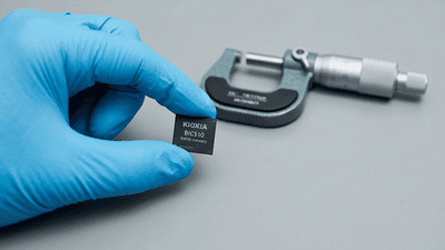
On July 3, 2026, Kioxia announced sample shipments of 1-terabit triple-level-cell devices using its tenth-generation BiCS FLASH technology. The company identified enterprise and data-center SSDs as the primary destination and planned production at its Kitakami Plant Fab2 facility in Iwate Prefecture, Japan. It also cautioned that sample specifications could differ from those of mass-produced devices.
The strategic theme is density, but not density alone. BiCS10 combines more layers with lateral scaling, interface improvements, and power-efficiency changes. Its value will ultimately be measured in usable enterprise-storage performance, not simply the height of the NAND stack.
Why 332 Layers Matter
Three-dimensional NAND increases storage density by arranging memory cells vertically as well as laterally. Adding layers can place more storage capability within a given footprint, helping manufacturers advance beyond the limitations of a purely planar design.
However, a layer count does not fully describe a NAND product. Cell layout, peripheral circuitry, die organization, bits per cell, and manufacturing yield all influence the resulting density and economics.
That distinction is central to BiCS10. Kioxia attributed the announced density improvement to both the 332-layer structure and better lateral density, rather than vertical stacking alone.
For investors, this makes the announcement more informative than a simple numerical contest. The competitive question is how efficiently a supplier converts its architecture into qualified bits and finished-storage products.
The Density Gain Has a Specific Comparison Basis

Sandisk’s parallel announcement described a 59% bit-density improvement and a 33% NAND-interface-speed increase relative to its eighth-generation 3D flash currently in mass production. The shared BiCS10 technology reached a stated density above 29 gigabits per square millimeter.
Those comparison details matter. The 59% figure should not be presented as an improvement over every previous generation or over every competing product.
Nor does it imply a 59% reduction in manufacturing cost. Higher density can support better economics, but processing complexity, capital investment, yield, and utilization also contribute to cost per usable bit.
From an analyst’s perspective, the proper reading is a substantial architectural density advance against a defined baseline—not a complete statement of future profitability.
A 1-Terabit Die Is Not a 1-Terabyte Drive
The sampled device has a nominal capacity of one terabit. That is approximately 125 gigabytes before considering the organization and overhead of a finished storage system.
A terabyte-scale SSD therefore combines multiple NAND dies with additional components and management functions. Its user capacity depends on how the drive allocates flash for data protection, internal management, and other purposes.
Triple-level-cell, or TLC, NAND stores three bits per memory cell. It should not be confused with a separately announced quad-level-cell product merely because both could use a related manufacturing platform.
For enterprise buyers, the distinction is practical. A NAND component establishes one part of the drive’s capability. It does not determine the finished SSD’s capacity, endurance, latency, or workload suitability by itself.
Kioxia and Sandisk Share the Technology Platform

Kioxia’s announcement was accompanied by Sandisk’s July 2 sampling announcement for BiCS10 1Tb TLC. The parallel releases reflect a shared development and manufacturing relationship, not two unrelated 332-layer technologies.
That shared foundation does not make the companies’ finished-storage portfolios identical. Controllers, firmware, product qualification, customer relationships, and system integration can create different commercial outcomes.
From a storage customer’s perspective, the relevant product is the drive that meets the application’s requirements. From an investor’s perspective, the relevant question is how each company turns the common NAND platform into differentiated revenue and returns.
BiCS10 therefore represents a shared manufacturing milestone with company-specific commercialization paths.
Sampling Opens the Qualification Process
Sample delivery allows engineers to evaluate the device’s behavior and begin integration work. It establishes that the technology has moved beyond an announcement of intent.
It does not establish broad availability or immediate high-volume deployment. Functional samples can support checks that precede final production specifications and customer qualification.
For an SSD developer, the work includes controller interaction, firmware development, error management, thermal behavior, and validation across relevant operating conditions.
The practical sequence runs from NAND evaluation to drive development, then to customer approval and recurring deployment. Each stage reduces uncertainty. Collapsing them into a claim that BiCS10 is already transforming enterprise shipments would bring future outcomes into the story too early.
Manufacturing Yield Determines the Economic Result
A denser architecture can be commercially attractive, but only if the manufacturer produces it with acceptable yields and costs.
Additional process complexity can increase the burden on fabrication, inspection, and control. Defects can reduce the number of usable dies, while variation can complicate qualification and product allocation.
This creates a difference between theoretical bit density and saleable output. The latter is what supports revenue.
For investors, the important milestones include stable manufacturing, improving yields, and successful customer deployment. A layer-count lead is less valuable if production remains expensive or unpredictable. Conversely, strong execution can make a technology commercially competitive even without the highest advertised layer count.
The Faster Interface Supports a Broader Performance Envelope
BiCS10’s announced NAND interface reaches up to 4.8 gigabits per second per data pin. That is a component-interface specification, not the sequential transfer rate of an entire SSD.
A drive’s performance also depends on its controller, channel arrangement, NAND parallelism, firmware, host interface, and workload.
The faster interface can give designers more bandwidth with which to build a product. It does not guarantee that every drive will run proportionately faster.
For enterprise systems, the value appears when the additional capability resolves a real bottleneck. If another part of the drive or platform remains limiting, the component improvement may have a smaller effect on the workload result.
Power Efficiency Matters at Data-Center Scale
Enterprise storage is judged partly by how much capacity and performance it provides within a power and cooling budget. That makes efficiency a commercial attribute rather than merely a specification-sheet improvement.
BiCS10’s announcements included improvements in read, write, and input-output power efficiency. These are device-level claims with defined operating conditions, not promises of equivalent reductions in total server electricity use.
The SSD controller and other components consume power, while the wider system includes processors, memory, networking, and cooling.
For a data-center operator, the useful question is the complete drive’s performance per watt under the intended workload. Better NAND efficiency contributes to that objective, but the system must demonstrate the benefit.
Enterprise SSDs Need Consistency as Well as Speed
Peak bandwidth attracts attention, but enterprise buyers also care about latency consistency, endurance, error handling, and behavior during sustained workloads.
A drive can perform well in a short benchmark while showing different characteristics after prolonged use or under mixed activity. Product qualification needs to reflect the conditions the customer expects to encounter.
That gives controller and firmware development a substantial role. NAND capabilities need to be managed within a complete storage product.
From an engineering perspective, BiCS10 expands the design opportunity. From a procurement perspective, the decisive evidence is the behavior of a qualified SSD—not the isolated memory device.
The DDR5 Connection Is Architectural, Not Technological
DDR5 is system memory based on DRAM, while NAND provides nonvolatile storage. They perform different functions and should not be treated as interchangeable capacity.
The BiCS10 announcement also refers to Toggle DDR6.0, a NAND interface specification. Despite the shared “DDR” terminology, that is not a successor module standard for DDR5 server memory.
The commercial connection lies in server architecture. DDR5 supports active working data, while enterprise SSDs hold persistent data and participate in storage workflows.
Increasing storage density does not automatically reduce the need for DDR5. The balance depends on software, workload, caching, and data movement. A system must be evaluated as a hierarchy rather than as a competition between memory technologies.
AI Creates Several Storage Requirements
AI-related storage demand includes datasets, checkpoints, retrieval information, logs, and other data used before, during, and after model execution.
Those activities do not all need the same storage characteristics. Some emphasize capacity, others throughput, and others response time or sustained write behavior.
Kioxia’s enterprise focus places BiCS10 within that varied demand environment. Higher density and efficiency can be attractive, but the finished product must match the workload.
For investors, “AI storage” is therefore a useful market description but an incomplete product thesis. The next questions concern which customers adopt the drives, which applications they serve, and whether the benefits justify deployment.
More Layers Do Not Guarantee a Market-Share Gain
NAND competition includes manufacturing cost, supply reliability, controller integration, customer qualification, and product execution. A numerical layer advantage addresses only part of that contest.
Customers may retain an established supplier because its products are already validated. Another supplier may compete through a different combination of cell architecture, capacity, endurance, or cost.
The result is a market in which several technologies can succeed in different applications.
For Kioxia, BiCS10’s significance will become clearer through commercial adoption and operating economics. Sampling is a meaningful entry point, but recurring shipments establish the competitive result.
The Supply Impact Will Arrive Gradually
A transition to denser NAND can increase bit output from manufacturing resources, but its market effect depends on the pace of the ramp.
Equipment readiness, process stability, yield, customer qualification, and demand allocation all influence when additional saleable bits become available.
Older generations can also remain important during the transition. Customers do not necessarily replace qualified products immediately because a newer component exists.
For analysts tracking NAND supply, the useful indicators are accepted output and actual product deployment. Treating sample delivery as a sudden supply increase can lead to premature conclusions about pricing and inventory.
What to Watch After the Sample Announcement
The most informative milestones connect technical capability with commercial scale.
- Confirmation of final production specifications and manufacturing progress.
- Evidence of stable yields and qualified output.
- Announcements of finished SSD products using the technology.
- Customer qualification and repeat enterprise deployments.
- Measured drive-level performance, endurance, and efficiency.
- The effect of product mix on revenue and profitability.
These indicators provide a stronger framework than forecasting sales from the layer count alone. They also distinguish a promising technology transition from an already realized earnings contribution.
The Layer Race Is Becoming a Systems Race
Kioxia’s 332-layer BiCS10 sample delivery is an important development in NAND density, interface capability, and efficiency. Its enterprise orientation makes the announcement especially relevant to data-center storage.
Yet the commercial test lies beyond the flash die. Controllers, firmware, qualification, manufacturing yield, and customer workloads determine how much of the technical advance becomes useful storage.
The next milestone is not simply a larger layer number. It is a qualified product that customers deploy repeatedly because it delivers better economics. That is where the NAND race becomes an enterprise-storage advantage.